- 您现在的位置:买卖IC网 > Sheet目录323 > DSP56311EVM (Freescale Semiconductor)KIT EVALUATION FOR DSP56311
�� �
�
�Enhanced� Filter� Coprocessor�
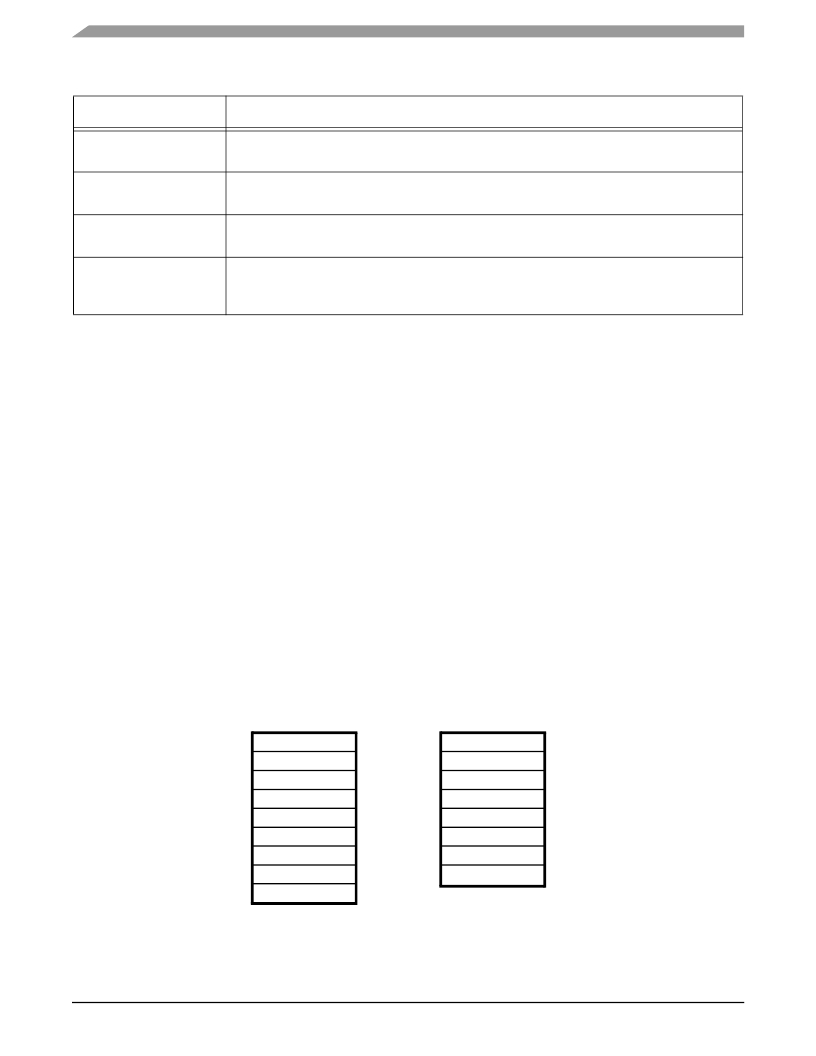
�Table� 10-1.� EFCOP� Registers� Accessible� Through� the� PMB� (Continued)�
�Register� Name�
�EFCOP� ALU� Control�
�Register� (FACR)�
�EFCOP� Data� Buffer� Base�
�Address� (FDBA)�
�EFCOP� Coefficient� Buffer�
�Base� Address� (FCBA)�
�Decimation/�
�Channel� Count� Register�
�(FDCH)�
�Description�
�A� 24-bit� read/write� register� used� by� the� DSP56300� core� to� program� the� EFCOP� data� ALU�
�operating� modes.�
�A� 16-bit� read/write� register� used� by� the� DSP56300� core� to� indicate� the� EFCOP� the� data� buffer�
�base� start� address� pointer� in� FDM� RAM.�
�A� 16-bit� read/write� register� by� which� the� DSP56300� core� indicates� the� EFCOP� coefficient� buffer�
�base� start� address� pointer� in� FCM� RAM.�
�A� 24-bit� register� that� sets� the� number� of� channels� in� multichannel� mode� and� the� filter�
�decimation� ratio.� The� EFCOP� address� generation� logic� uses� this� information� to� supply� the�
�correct� addressing� to� the� FDM� and� FCM.�
�10.2.2� EFCOP� Memory� Banks�
�The� EFCOP� contains� two� memory� banks:�
�Filter� Data� Memory� (FDM).� This� 24-bit-wide� memory� bank� is� mapped� as� X� memory� and�
�stores� input� data� samples� for� EFCOP� filter� processing.� The� FDM� is� written� via� a� 4-word�
�FIFO� (FDIR),� and� its� addressing� is� generated� by� the� EFCOP� address� generation� logic.� The�
�input� data� samples� are� read� sequentially� from� the� FDM� into� the� MAC.� The� FDM� is�
�accessible� for� writes� by� the� core,� and� the� DMA� controller� and� is� shared� with� the� 12� K�
�lowest� locations� ($0–$2FFF)� of� the� on-chip� internal� X� memory.�
�Filter� Coefficient� Memory� (FCM)� .� This� 24-bit-wide� memory� bank� is� mapped� as� Y�
�memory� and� stores� filter� coefficients� for� EFCOP� filter� processing.� The� FCM� is� written� via�
�the� DSP56300� core,� and� the� EFCOP� address� generation� logic� generates� its� addressing.� The�
�filter� coefficients� are� read� sequentially� from� the� FCM� into� the� MAC.� The� FCM� is�
�accessible� for� writes� only� by� the� core.� The� FCM� is� shared� with� the� 12� K� lowest� locations�
�($0–$2FFF)� of� the� on-chip� internal� Y� memory.�
�Note:�
�The� filter� coefficients,� H(n),� are� stored� in� “reverse� order,”� where� H(N� –� 1)� is� stored� at�
��D(0)�
�D(1)�
�D(2)�
�H(N� -� 1)�
�H(N� -� 2)�
�-�
�Data�
�Memory�
�Bank�
�(FDM)�
�D(3)�
�D(4)�
�D(5)�
�-�
�-�
�-�
�-�
�-�
�H(1)�
�H(0)�
�Coefficient�
�Memory�
�Bank�
�(FCM)�
�Figure� 10-2.� Storage� of� Filter� Coefficients�
�DSP56311� Reference� Manual,� Rev.� 2�
�10-4�
�Freescale� Semiconductor�
�发布紧急采购,3分钟左右您将得到回复。
相关PDF资料
DSPAUDIOEVMMB1E
BOARD MOTHER DSP563XX
DSPIC30F2010 DEVELOPMENT KIT
KIT DEV EMBEDDED C
DSTRM-KT-0181A
DSTREAM DEBUG AND TRACE UNIT
DSUT1CSU
SURGE SUPPR NETWORK W/GROUND
DTEL2
SURGE SUPPRESSOR PHONE RJ11/RJ45
DV003001
PROGRAMMER PICSTART PLUS 16C/17C
DV164035
MPLAB ICD3 IN-CIRC DEBUGGER
DV164039
KIT DEV PIC24FJ256DA210
相关代理商/技术参数
DSP56311EVMIG_D
制造商:未知厂家 制造商全称:未知厂家 功能描述:DSP56311EVMIG DSP56311EVM Sample Code
DSP56311EVMUM
制造商:未知厂家 制造商全称:未知厂家 功能描述:DSP56311 Evaluation Module Hardware Reference Manual
DSP56311FACT
制造商:未知厂家 制造商全称:未知厂家 功能描述:DSP56311 Higher performance programmable DSP for demanding voice and data applications
DSP56311UM
制造商:未知厂家 制造商全称:未知厂家 功能描述:DSP56311 24-Bit Digital Signal Processor Users Manual
DSP56311UMAD
制造商:未知厂家 制造商全称:未知厂家 功能描述:DSP56311 Users Manual Addendum
DSP56311VF150
功能描述:数字信号处理器和控制器 - DSP, DSC 150Mhz/300MMACS 150Mhz EFCOP RoHS:否 制造商:Microchip Technology 核心:dsPIC 数据总线宽度:16 bit 程序存储器大小:16 KB 数据 RAM 大小:2 KB 最大时钟频率:40 MHz 可编程输入/输出端数量:35 定时器数量:3 设备每秒兆指令数:50 MIPs 工作电源电压:3.3 V 最大工作温度:+ 85 C 封装 / 箱体:TQFP-44 安装风格:SMD/SMT
DSP56311VF150B1
功能描述:数字信号处理器和控制器 - DSP, DSC 24 BIT DSP
RoHS:否 制造商:Microchip Technology 核心:dsPIC 数据总线宽度:16 bit 程序存储器大小:16 KB 数据 RAM 大小:2 KB 最大时钟频率:40 MHz 可编程输入/输出端数量:35 定时器数量:3 设备每秒兆指令数:50 MIPs 工作电源电压:3.3 V 最大工作温度:+ 85 C 封装 / 箱体:TQFP-44 安装风格:SMD/SMT
DSP56311VF150R2
功能描述:数字信号处理器和控制器 - DSP, DSC 24 BIT DSP RoHS:否 制造商:Microchip Technology 核心:dsPIC 数据总线宽度:16 bit 程序存储器大小:16 KB 数据 RAM 大小:2 KB 最大时钟频率:40 MHz 可编程输入/输出端数量:35 定时器数量:3 设备每秒兆指令数:50 MIPs 工作电源电压:3.3 V 最大工作温度:+ 85 C 封装 / 箱体:TQFP-44 安装风格:SMD/SMT